PEAK HOLD DETECTOR PH300

STATE-OF-THE-ART PERFORMANCE
? High Speed (250 ns rise time)
? Extremely Low Droop Rate (10 nV/ms)
? Low Power (<36 mW)

? Ramp & Dump Hold Discharge


立即咨詢
產(chǎn)品詳情


  Amptek Model PH300 is a high performance, thin film hybrid, peak-hold unit, designed to track and hold the peak of analog input signals with rise times (10% to 90% of Vmax) as short as 250 ns. The unit also has the lowest Droop Rate of the held voltage available and consumes less than 36 mW of power in quiescent mode.

   While this unit was designed for use in satellite instrumentation, the following unique characteristics make it equally useful in a broad range of space, laboratory and commercial applications.

FEATURES
APPLICATIONS
? Operates from -55 °C to +125 °C
? Aerospace
? Small size (16 pin hybrid DIP)
? Portable instrumentation
? Very low power (36 mW quiescent)
? Nuclear monitoring
? High speed
? Particle, x-ray and gamma ray detection
? Low droop rate
? Imaging
? Ramp discharge
? Research experiments
? Fast reset
? Medical and nuclear electronics
? Build-in linear gate
? Electro-optical systems
? Internal hold capacitor

? High reliability screening

? One year warranty


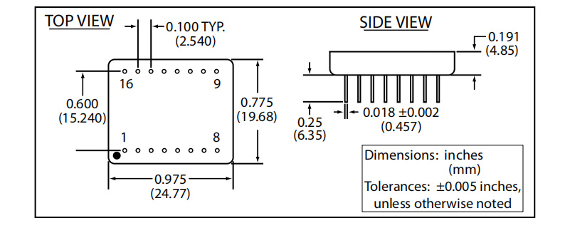
PH300 Mechanical Diagram


SPECIFICATIONS

INPUT CHARACTERISTICS
Signal -Analog
Range: 0 to (V+- 1.5V)
Input impedance: >1 k?
Rise time (10% - 90%): 250 ns (min)
Linear Gate Control -Digital
Logic level: TTL
Gate open: HIGH
Gate closed: LOW
Gate turn on/off: 40 ns (60 ns max)
Reset Control- Digital
Ramp slew rate: 5 V/μs to 0.001 V/μs
Ramp control: TTL
Ramp active: LOW
Fast reset: <800 ns (dump mode)
Dump control: TTL
Dump active: LOW
OUTPUT CHARACTERISTICS
Analog
Range-load: >5 k?: 0 to (V+- 1.5 V)(typical)
Output slew rate: 30 V/μs
Droop rate: <100 nV/μs @ 25 °C
                 <5 μV/μs @ 70 °C
Linearity: ±0.01% (typical)
DC offset: ±2 mV (max)
Output current: Internally limited to15 mA
Digital Peak Detect
Logic level: TTL
Vin > Vout : HIGH
Vin < Vout: LOW
Propagation delay: <500 ns (typical)
Hold Capacitor
Internal: 470 pF ±5%
External: 50 pF - 1000 pF (optional)
ENVIRONMENT
Case Temperature
Operating: -55 °C to +125 °C
Storage: -55 °C to +150 °C
Radiation
Hardness: 105rad(Si) (optional withPH300RH only)
Screening
Amptek High Reliability
Power Supply
Quiescent power: <36 mW @ -5V/+10V
Analog
V+: +5 V to +12 V (absolute maximum 18V)
Vˉ: -5 V to -6 V (absolute maximum (V+- Vˉ) <30 V)
Quiescent I+: <2.4 mA (-55 °C to +125 °C)
Quiescent Iˉ: <2.4 mA (-55 °C to +125 °C)
Digital
Vd : +5 V (absolute maximum +7 V)
Quiescent Id : <0.01 mA (-55 °C to +125 °C)
Package
Hermetic, 16 pin hybrid, 600 mil DIP

PIN DESCRIPTION
PIN
DESCRIPTION
1
IN is the analog input of the PH300. This input accepts a positive signal. The input signal should not be driven greater than the positive analog power supply, or less than -0.5 V. Schottky diode input protection is recommended.
2
V- (-5 V to -6 V)
3
RCEXT is a node that allows connection of an external hold resistor and hold capacitor.When internal hold components are used, RCEXT is left unconnected.
4
HRES is the node of the internal hold resistor.
5
HCAP is the node of the internal hold capacitor. This node is normally connected to HRES and DSCHG.
6
DSCHG is a node of the current generator used to reset the hold capacitor of the PH300. The RAMP reset current is set by an external current source or an external resistor. This node is in a high impedance state when PH300 is in hold mode. Normally this node is connected to the HCAP node.
7
ISET is a node of the current mirror that sets the discharge current. This node sinks positive current. The discharge current is twice the current at this node. An external resistor R can be connected between ISET and ground. In this case the reset current is approximately set to: 2*(Vˉ+ 0.6 V)/(R + 500 Ω). Amptek recommends a minimum value of 1 k for the external resistor.
NOTE! To ensure proper PH300 tracking mode operation, a reset current must be set regardless of the reset scheme (RAMP or DUMP) used to discharge the hold capacitor.
8
GND
9
DUMP (active low) is a TTL compatible signal used for fast reset of the PH300. This signal must be used only in conjunction with the RAMP signal. The DUMP signal can be active only when RAMP is active. A LOW state of this signal causes the discharge current to peak up to 20 mA, causing fast discharge of the hold capacitor. The duration of the DUMP signal should be keep as short as possible, since the high reset current increases substantially the power consumption of the PH300. A fixed duration of 1μs usually is sufficient to completely reset the built in hold capacitor. The PKDT signal can be used as an indicator for the discharge of the hold capacitor and may provide a function to control the duration of the DUMP signal.
10
RAMP (active low) is a TTL compatible input that controls the linear discharge of the PH300. When this signal is LOW, the DSCHG node sinks current that resets the hold capacitor. Since the reset current is constant, the output of PH300 decays linearly.
11
GATE (open high) is a TTL compatible logic input that controls the linear gate of the PH300. When GATE is in an active HIGH state, the linear gate is open and the error amplifier of the PH300 can sense the input signal. When GATE is inactive, the error amplifier input is tied to ground.
12
PKDT is an TTL output that indicates the state of the PH300. When this signal is LOW, the PH300 is in a hold mode.
13
Vd (+5 V)
14
V+(+5 V to +12 V)
15
COMP is a node for frequency compensation of the PH300 when an external hold capacitor is used. In this case a resistor between 20 and 100 Ω can be used to reduce output signal oscillations. This resistor must be connected between COMP and V+When the internal hold capacitor is used, COMP must be connected to V+.
16
OUT is the analog output of the PH300. This output is protected for short circuits to ground or any voltage between ground and the positive analog power supply.WARNING! Shorting this output to any negative voltage may destroy the PH300 circuit.This output can drive capacitive loads up to 50 pf (typical). For higher capacitive loads,use a resistor of 50 to 100 Ω in series with OUT. Range is 0 to (V+- 1.5 V), typical.

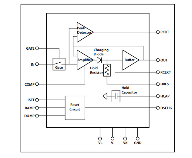
FUNCTIONAL DIAGRAM


PRINCIPLE OF OPERATION
   The PH300 is a peak-hold device, designed to track an analog input pulse and keep the maximum amplitude as a peak voltage on a hold capacitor. Major functional elements are
identified in the functional diagram above. An innovative boot-strap circuit in the input stage of the output buffer amplifier, minimizes the droop error which occurs during periods of long peakhold duration.
   Inputs to the IN terminal are gated through a linear gate (gate input), which is controlled by a TTL compatible logic signal.When the gate is open (gate high), the input signal is sensed
by the error amplifier. When the gate is closed (gate low), the input to the error amplifier is grounded and the input signal does not have any effect on the output of PH300.
   During the rise time of the input signal, the hold capacitor is charged through a charging diode and a hold resistor. For the PH300, this mode of operation is referred to as the charging
mode. The device goes into hold mode as soon as the input reaches Vmax and starts to decay. This state can be terminated by discharging the hold capacitor. When the circuitry to ac
complish this is enabled, the PH300 is placed in discharge mode. A special case of the discharge mode is the tracking mode. Additional information on each of these operational
modes follows.
CHARGING MODE
   The hold capacitor is charged during the rise time of the input signal. The rise time of the input pulses can be as short as 250 ns. When the PH300 is in charging mode, negative feedback is applied to the amplifier through the high impedance output buffer. Under this condition, the output voltage follows the input signal and the peak-detector logic output is in the inactive state. The feedback circuit brakes immediately after the input goes through a maximum level and starts decaying.The PH300 then enters hold mode.

PRINCIPLE OF OPERATION (con’t)
HOLD MODE
   In this mode, the charging diode is reverse biased and the voltage across the hold capacitor is held equal to Vmax. The peak-detector logic output is in the active state. The leakage
currents of the components connected to the hold capacitor causes it to discharge. The rate of this discharge is the droop rate of the PH300.
DISCHARGE MODE
   The hold capacitor could be intentionally discharged by enabling the reset circuit within the PH300. Two types of reset are possible. They are: (i) ramp or linear reset and (ii) dump or fast reset.
   In ramp discharge mode, the hold capacitor is discharged through a constant current draw, which is set with an external resistor or by an external current source. Constant current
discharge results in a linear decrease of the held voltage. This operating mode is used in Wilkinson type analog to digital converters.
   In fast discharge mode, the hold capacitor is discharged through a large current draw for a short period of time. The frequency and duration of this mode of operation determines the upper limit of power consumption for the device.
TRACKING MODE
   Negative feedback to the amplifier could become active (and correspondingly the peak-detector logic output goes to the inactive state) in discharge mode operation, if the hold
capacitor voltage becomes less than or equal to the voltage at the amplifier input. Therefore, if the discharge rate of the hold capacitor is higher than the decay rate of the input signal, the output of the PH300 will follow the input even when the signal is decaying. This mode of PH300 operation is referred to as the tracking mode.
INPUT PROTECTION - CAUTION
   The input (Pin 1) of the PH300 connects internally directly to an input of a CD4066 Quad Bilateral Switch. Vdd, the positive supply for this chip, connects to V+ (+5 to +12V), Pin 14 of the PH300 and Vss connects to GND, Pin 8. Normal precautions for the use of the CD4066 must be observed with the PH300 to avoid damage. These precautions include keeping the input voltage within (Vss - 0.5V) and (Vdd + 0.5V).
   In particular, care should be taken that these conditions are not violated on power-up or power-down,or when a connector is mated or de-mated with power on.
   Input protection can be provided by a current-limiting resistor (>200 Ω) in series with the input, or by connecting a diode from the input (Pin1) to ground (Pin 8), with anode grounded.


APPLICATION NOTES


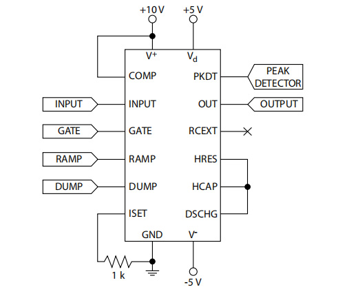
Figure 1. - PH300 typical wiring diagram.
   Figure 1 shows a typical wiring diagram of PH300 using the internal hold and reset components. The board design should prevent any possible paths for leakage currents to
the DSCHG, HCAP, HRES and RCEXT nodes.


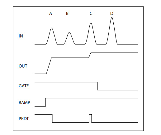
Figure 2. - Gate function of PH300.
   Figure 2 shows the use of the linear gate. Four pulses marked A, B, C, and D are applied to the input of PH300. The linear gate is open for the first three pulses and closed for the last
pulse, D. The PH300 is not discharged between the pulses.Only the peaks of the pulses A and C will be detected. Pulse B passes through the linear gate. However, since its amplitude
is less than the held amplitude of pulse A, there is no change of the PH300 output. Pulse D does not affect the held peak voltage of pulse C because the linear gate is closed.


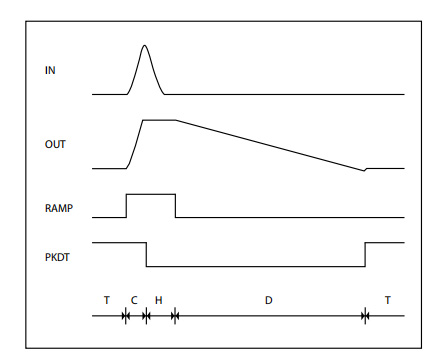
Figure 3. - Timing diagram illustrating RAMP
reset of PH300.


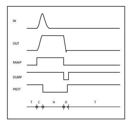
Figure 4. - Timing diagram illustrating DUMP
reset of PH300.
Figures 3 and 4 illustrate the modes of operation of the PH300 with RAMP and DUMP reset of the hold capacitor. The linear gate is open. The modes of operation are indicated with bold characters as follows:
     C = charging mode
     D = discharge mode
     H = hold mode
     T = tracking mode


Copyright? 安徽省科華貿(mào)易有限責(zé)任公司 版權(quán)所有 皖I(lǐng)CP備18022818號-1
地址:安徽省合肥市高新區(qū)昌河科創(chuàng)大廈702室電話:0551-65392835郵箱:service@kehua-trade.com
Designed by Wanhu
微信二維碼
国产成人亚洲影院,成人永久免费福利视频APP,成人女性爽爽影院,国外人成人色视频在线